| CPC H10K 50/844 (2023.02) [H10K 50/841 (2023.02); H10K 59/12 (2023.02); H10K 59/8722 (2023.02); H10K 71/00 (2023.02); H10K 77/111 (2023.02); H10K 59/122 (2023.02); H10K 59/124 (2023.02); H10K 59/873 (2023.02); H10K 71/851 (2023.02); H10K 2102/311 (2023.02); Y02E 10/549 (2013.01); Y02P 70/50 (2015.11)] | 20 Claims |

|
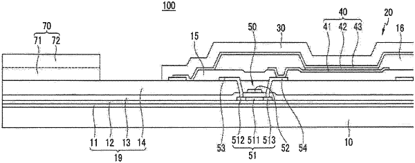
[ 18. A flexible display, comprising:
a flexible substrate;
a transistor disposed on the flexible substrate and including a semiconductor layer, a gate electrode, a source electrode, and a drain electrode;
a plurality of inorganic layers including a barrier layer, a buffer layer, a gate insulating layer, and an interlayer insulating layer sequentially disposed on the flexible substrate;
a light emitting element disposed on the interlayer insulating layer and electrically connected to the transistor;
a thin film encapsulation layer covering the light emitting element; and
a crack suppressing layer disposed directly on the interlayer insulating layer and along an edge of the flexible substrate,
wherein at least one of the barrier layer and the buffer layer is disposed at the edge of the flexible substrate,
wherein at least one of an edge of the gate insulating layer and an edge of the interlayer insulating layer is spaced apart from the edge of the flexible substrate. ]
|