| CPC H10N 70/24 (2023.02) [H10B 63/34 (2023.02); H10B 63/845 (2023.02); H10N 70/8833 (2023.02)] | 20 Claims |
|
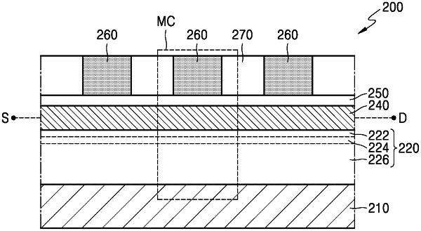
1. A variable resistance memory device comprising:
an insulating layer;
a variable resistance layer on the insulating layer;
a channel layer on the variable resistance layer;
a gate insulating layer on the channel layer; and
a plurality of gate electrodes on the gate insulating layer,
wherein the plurality of gate electrodes are spaced apart from each other,
wherein the variable resistance layer includes a first oxide layer, a second oxide layer, and a third oxide layer sequentially arranged on the insulating layer, and
wherein a dielectric constant of the second oxide layer is greater than a dielectric constant of the first oxide layer and a dielectric constant of the third oxide layer.
|