US 11,856,865 B2
Gradient protection layer in MTJ manufacturing
Tai-Yen Peng, Hsinchu (TW); Yu-Shu Chen, Hsinchu (TW); Sin-Yi Yang, Taichung (TW); Chen-Jung Wang, Hsinchu (TW); Chien Chung Huang, Taichung (TW); Han-Ting Lin, Hsinchu (TW); Jyu-Horng Shieh, Hsinchu (TW); and Qiang Fu, Hsinchu (TW)
Assigned to Taiwan Semiconductor Manufacturing Company, Ltd., Hsinchu (TW)
Filed by Taiwan Semiconductor Manufacturing Co., Ltd., Hsinchu (TW)
Filed on Jul. 20, 2022, as Appl. No. 17/869,335.
Application 17/120,613 is a division of application No. 16/170,750, filed on Oct. 25, 2018, granted, now 10,868,239, issued on Dec. 15, 2020.
Application 17/869,335 is a continuation of application No. 17/120,613, filed on Dec. 14, 2020, granted, now 11,411,176.
Prior Publication US 2022/0367794 A1, Nov. 17, 2022
This patent is subject to a terminal disclaimer.
Int. Cl. H10N 50/01 (2023.01); H10N 50/80 (2023.01)
CPC H10N 50/01 (2023.02) [H10N 50/80 (2023.02)] 20 Claims
OG exemplary drawing
 
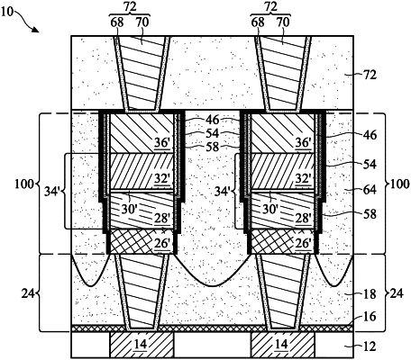
1. A device comprising:
a Magnetic Tunnel Junction (MTJ) stack comprising:
a bottom electrode;
a bottom magnetic electrode over the bottom electrode;
a tunnel barrier over the bottom magnetic electrode;
a top magnetic electrode over the tunnel barrier; and
a top electrode over the top magnetic electrode; and
a dielectric protection layer extending onto a sidewall of the MTJ, wherein the dielectric protection layer comprises:
a first portion;
a second portion lower than and joined to the first portion; and
a third portion lower than and joined to the second portion, wherein the first portion, the second portion, and the third portion have different thicknesses.