| CPC H10N 50/01 (2023.02) [H01F 10/3254 (2013.01); H01F 41/34 (2013.01); H10N 50/10 (2023.02); H10N 50/80 (2023.02); H10B 61/00 (2023.02)] | 20 Claims |
|
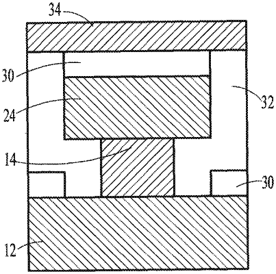
1. A device comprising:
a first electrode;
a first conductive feature interfacing with the first electrode, the first conductive feature having a first width in a first direction;
a second conductive feature interfacing with the first conductive feature, the second conductive feature having a second width in the first direction that is different than the first width, wherein the second conductive feature has a top surface facing away from the first electrode;
a first magnetic tunneling junction (MTJ) structure interfacing with the second conductive feature and extending to a first height over the first electrode, wherein the first MTJ structure completely covers the top surface of the second conductive feature;
a second MTJ structure interfacing with the first electrode and extending to a second height over the first electrode, the second height being different than the first height; and
a dielectric layer extending continuously from the second MTJ structure to the first conductive feature.
|