| CPC H10K 71/00 (2023.02) [H10K 59/1201 (2023.02); H10K 59/122 (2023.02); H10K 71/80 (2023.02); H10K 2102/311 (2023.02)] | 16 Claims |
|
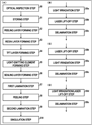
1. A method for manufacturing a display device including a light-emitting element, the method comprising:
storing, in a manufacturing process of the display device, a plurality of abutting positions where a back face of a support substrate locally abuts a manufacturing apparatus;
forming, on a surface of the support substrate on a side on which the light-emitting element is to be formed, a peeling layer at a position opposing at least one position of the plurality of abutting positions stored;
forming, on the support substrate, a resin layer to cover the peeling layer;
forming a TFT layer on the resin layer;
forming the light-emitting element on the TFT layer; and
peeling the support substrate and the resin layer.
|