| CPC H10K 59/131 (2023.02) [H01L 24/29 (2013.01); H01L 24/83 (2013.01); H01L 2224/29239 (2013.01); H01L 2224/29244 (2013.01); H01L 2224/29247 (2013.01); H01L 2224/29255 (2013.01); H01L 2224/29257 (2013.01); H01L 2224/83851 (2013.01); H01L 2224/83862 (2013.01); H01L 2924/12044 (2013.01); H10K 59/1201 (2023.02)] | 17 Claims |
|
1. A method of manufacturing a display device, the method comprising:
providing a lower substrate having a display area and a pad area;
forming a display structure in the display area of the lower substrate;
forming pad electrodes in the pad area of the lower substrate to be spaced apart from each other in a first direction parallel to a top surface of the lower substrate;
forming an upper substrate on the display structure to face the lower substrate in the display area;
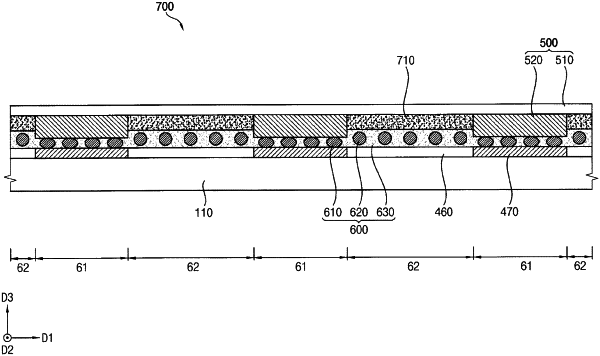
forming a conductive film member including a non-cured resin layer and conductive balls arranged in a lattice shape on the pad electrodes, the non-cured resin layer overlapping the pad electrodes;
forming a film package on the non-cured resin layer, the film package including bump electrodes overlapping the pad electrodes; and
placing a pre-cured resin on one side of the pad electrodes,
wherein at least a portion of the pre-cured resin directly contacts a side surface of the bump electrodes.
|