| CPC H10K 59/131 (2023.02) | 12 Claims |
|
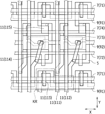
1. A display device displaying an image by supplying corresponding data signals to a plurality of pixel circuits arranged in a display panel, the display device comprising:
a semiconductor layer; a gate insulating film; a first display wire; a first interlayer insulating film; a second display wire; a second interlayer insulating film; and a third display wire stacked on a substrate in this order,
the first display wire including a plurality of scanning signal lines extending in a row direction,
the second display wire including a plurality of constant potential wires extending in the row direction,
the third display wire including a plurality of data signal lines extending in a column direction and intersecting with the scanning signal lines and the constant potential wires, the column direction intersecting with the row direction,
the plurality of pixel circuits provided corresponding to intersections of the data signal lines and the scanning signal lines,
each of the pixel circuits including a first transistor and a second transistor in which any one of the scanning signal lines overlaps the semiconductor layer on top of the gate insulating film,
one conductive terminal of the first transistor and one conductive terminal of the second transistor being connected together through a connector included in a conductor region of the semiconductor layer, and
the connector including an overlap connector overlapped in a plan view with the data signal lines through the constant potential wires.
|