| CPC H10K 59/131 (2023.02) [H10K 59/1213 (2023.02); H10K 59/1216 (2023.02); H01L 27/1214 (2013.01)] | 17 Claims |
|
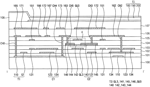
1. A display device comprising:
a first active layer disposed on a substrate;
a scan line disposed on the first active layer;
a lower gate electrode disposed on the scan line;
a second active layer disposed on the lower gate electrode, the second active layer including an oxide semiconductor pattern that includes a channel overlapping the lower gate electrode and a low-resistance part formed on a side portion of the channel;
a metal pattern disposed on at least one surface of the low-resistance part; and
an upper gate electrode disposed on the second active layer to overlap the channel,
wherein the low-resistance part is electrically connected to the first active layer.
|