| CPC H10K 59/131 (2023.02) [H01L 27/1214 (2013.01); H10K 50/131 (2023.02); H10K 50/805 (2023.02); H10K 59/1795 (2023.02); H10K 50/8426 (2023.02)] | 19 Claims |
|
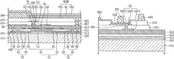
1. An organic light emitting display device, comprising:
a substrate comprising a display area and a non-display area;
an organic light emitting element comprising a first electrode, an organic light emitting layer (OL) over the first electrode, and a second electrode over the organic light emitting layer, wherein the first electrode is at the display area of the substrate;
a gate line and a data line on the substrate;
a thin film transistor connected to the gate line and the data line;
an insulating layer over the thin film transistor;
a first conductive line on the insulating layer at the non-display area of the substrate;
a first organic layer on the first conductive line; and
a second conductive line, wherein at least a part of the second conductive line is on the first organic layer and connected to the first conductive line,
wherein the second conductive line is connected to the second electrode,
wherein the first organic layer has a contact hole, and
the second conductive line is connected to the first conductive line through the contact hole.
|