| CPC H10K 59/123 (2023.02) [G09G 3/3233 (2013.01); H10K 59/124 (2023.02); H10K 59/131 (2023.02); H10K 59/40 (2023.02); H10K 59/88 (2023.02); G06F 3/0446 (2019.05); G06F 3/04164 (2019.05); G09G 2300/0426 (2013.01)] | 19 Claims |
|
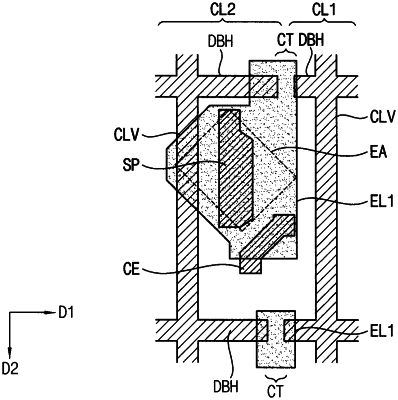
1. A display device comprising:
a first display area and a second display area adjacent to the first display area in a first direction;
pixel circuits, each of the pixel circuits including at least one transistor;
light-emitting elements including a pixel electrode electrically connected to a corresponding one of the pixel circuits;
signal wirings that transfer a driving signal to the pixel circuits; and
connection wirings that transfer a driving signal to signal wirings disposed in the second display area, at least one of the connection wirings including:
a first connection wiring extending in the first direction; and
a second connection wiring extending in a second direction,
wherein at least one of the first connection wiring and the second connection wiring has a disconnection portion, and
at least one of the pixel electrode overlaps the disconnection portion.
|