| CPC H10K 59/123 (2023.02) [H10K 59/00 (2023.02); H10K 71/00 (2023.02); H10K 59/1201 (2023.02)] | 12 Claims |
|
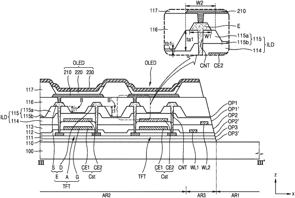
1. A display apparatus comprising:
a semiconductor layer on a substrate;
a gate insulating layer on the substrate and covering the semiconductor layer;
a gate electrode on the gate insulating layer and at least partially overlapping the semiconductor layer;
a first interlayer insulating layer on the gate electrode;
a second interlayer insulating layer on the first interlayer insulating layer;
an electrode layer on the second interlayer insulating layer and extending from a top surface of the second interlayer insulating layer to the semiconductor layer to be electrically connected to the semiconductor layer;
a pixel electrode disposed on the second interlayer insulating layer and electrically connected to the electrode layer; and
a pixel-defining layer disposed on an edge of the pixel electrode and exposing a center of the pixel electrode,
wherein the second interlayer insulating layer comprises:
a first portion;
a second portion extending from the first portion and vertically overlapping with the center of the pixel electrode; and
a third portion extending from the first portion and vertically overlapping with the pixel-defining layer,
the electrode layer is on the first portion of the second interlayer insulating layer,
a first step is provided by a difference in thicknesses of the first portion and the second portion,
a second step is provided by a difference in thicknesses of the first portion and the third portion, and
the second step is greater than the first step.
|