| CPC H10K 59/122 (2023.02) [G06F 3/0446 (2019.05); H10K 50/86 (2023.02); H10K 59/40 (2023.02)] | 11 Claims |
|
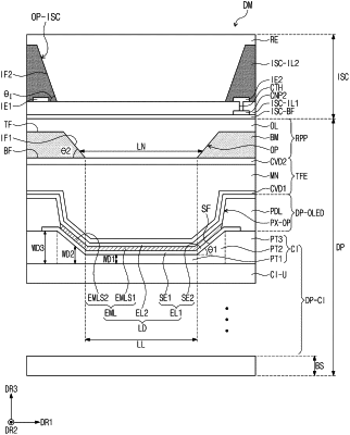
1. A display module comprising:
a base layer;
a circuit insulating layer disposed on the base layer;
a pixel definition layer disposed on the circuit insulating layer and including a pixel opening;
an emission layer disposed on the pixel opening;
encapsulation layer disposed on the emission layer;
a partition wall disposed on the encapsulation layer; and
an input sensing circuit disposed on the partition wall,
wherein the input sensing circuit comprises:
a first insulating layer,
a plurality of sensors disposed on the first insulating layer, and
a second insulating layer covering the plurality of sensors and including a touch opening, and
wherein the second insulating layer, the partition wall, and the pixel definition layer overlap in a plan view.
|