| CPC H10K 59/1213 (2023.02) [H10K 50/844 (2023.02); H10K 59/126 (2023.02); H10K 59/1216 (2023.02); H10K 59/131 (2023.02); H01L 27/124 (2013.01); H01L 27/1225 (2013.01); H01L 27/1255 (2013.01); H01L 29/7869 (2013.01); H01L 29/78633 (2013.01); H01L 29/78675 (2013.01)] | 17 Claims |
|
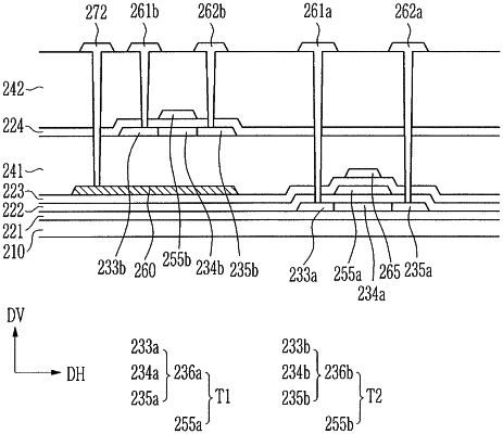
1. An organic light emitting diode display, comprising:
a substrate;
a first buffer layer on the substrate;
a first semiconductor layer on the first buffer layer;
a first gate insulating layer on the first semiconductor layer;
a first gate electrode on the first gate insulating layer;
a second gate insulating layer on the first gate electrode;
a second gate electrode and a blocking layer on the second gate insulating layer;
a second buffer layer on the second gate electrode and the blocking layer;
a second semiconductor layer on the second buffer layer, the second semiconductor layer including a channel region;
a third gate insulating layer on the second semiconductor layer; and
a third gate electrode on the third gate insulating layer, wherein
the blocking layer is disposed in a same layer as the second gate electrode, the blocking layer overlapping the channel region of the second semiconductor layer in a direction perpendicular to a surface of the substrate.
|