| CPC H10K 59/1213 (2023.02) [H10K 59/1216 (2023.02); H10K 71/00 (2023.02); H10K 77/10 (2023.02); H01L 27/1255 (2013.01); H01L 27/1259 (2013.01); H01L 28/60 (2013.01); H10K 59/1201 (2023.02)] | 15 Claims |
|
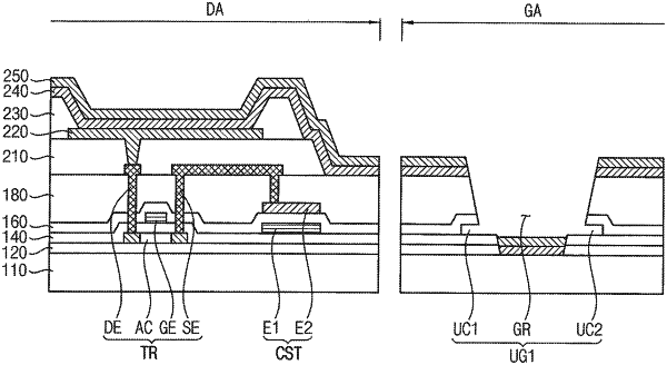
1. A display device comprising:
a substrate;
an organic light emitting layer overlapping the substrate; and
an insulating layer positioned between the substrate and the organic light emitting layer,
wherein a first through hole is formed through the organic light emitting layer, the insulating layer, and the substrate,
wherein an undercut-groove is formed through the organic light emitting layer and the insulating layer near the first through hole, and
wherein the undercut-groove comprises a first groove that surrounds the first through hole in a plan view of the display device and a first undercut that surrounds the first groove in the plan view of the display device.
|