| CPC H10K 50/865 (2023.02) [H10K 71/00 (2023.02); H10K 2102/102 (2023.02); H10K 2102/103 (2023.02)] | 17 Claims |
|
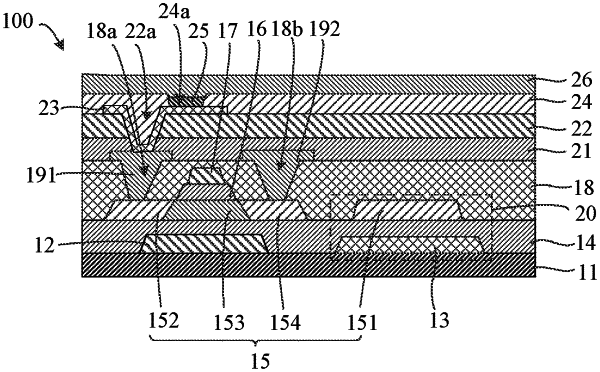
1. A display panel, comprising:
a substrate;
a light-shielding metal block and a transparent conductive block disposed on the substrate;
a buffer layer disposed on the substrate, the light-shielding metal block, and the transparent conductive block;
an active layer pattern disposed on the buffer layer, wherein the active layer pattern comprises a first conductive block, the first conductive block is disposed opposite to the transparent conductive block, the first conductive block is conductively formed by a semiconductor material, and the transparent conductive block and the first conductive block constitute two electrodes of a capacitor; and
a pixel electrode disposed on the active layer pattern, wherein an orthographic projection of the pixel electrode on the substrate is spaced apart from an orthographic projection of each of the transparent conductive block and the first conductive block on the substrate.
|