US 11,856,811 B2
Top emitting AMOLED display panel, manufacturing method thereof, and display device
Zhilin Zheng, Guangdong (CN); Jia Tang, Guangdong (CN); and Xiaoxing Zhang, Guangdong (CN)
Assigned to Shenzhen China Star Optoelectronics Semiconductor Display Technology Co., Ltd., Shenzhen (CN)
Appl. No. 17/056,436
Filed by Shenzhen China Star Optoelectronics Semiconductor Display Technology Co., Ltd., Guangdong (CN)
PCT Filed Oct. 22, 2020, PCT No. PCT/CN2020/122680
§ 371(c)(1), (2) Date Nov. 18, 2020,
PCT Pub. No. WO2022/047915, PCT Pub. Date Mar. 10, 2022.
Claims priority of application No. 202010928470.X (CN), filed on Sep. 7, 2020.
Prior Publication US 2022/0310968 A1, Sep. 29, 2022
Int. Cl. H01L 29/08 (2006.01); H10K 50/844 (2023.01); H10K 50/86 (2023.01); H10K 71/00 (2023.01); H10K 102/00 (2023.01)
CPC H10K 50/844 (2023.02) [H10K 50/86 (2023.02); H10K 71/00 (2023.02); H10K 2102/00 (2023.02); H10K 2102/3026 (2023.02)] 20 Claims
OG exemplary drawing
 
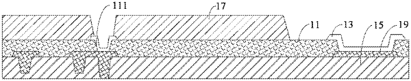
1. A top emitting active-matrix organic light-emitting diode (AMOLED) display panel, comprising a passivation layer and a protective conductive layer;
wherein the passivation layer is sandwiched between an interlayer insulating layer and a planarization layer of the top emitting AMOLED display panel, openings corresponding to a metal layer are defined in the passivation layer, and the metal layer is a metal layer formed on the interlayer insulating layer; and
wherein the protective conductive layer covers the metal layer and side walls of the openings, and a part of the protective conductive layer extends to the passivation layer.