| CPC H10K 50/844 (2023.02) [H10K 71/00 (2023.02); H10K 77/10 (2023.02); H10K 50/81 (2023.02); H10K 59/1201 (2023.02); H10K 59/122 (2023.02); H10K 59/124 (2023.02)] | 12 Claims |
|
1. A display panel, comprising:
a substrate, comprising a display area;
a backplane film layer, on a side of the substrate and in the display area;
a via hole, in the display area and completely running through the display panel along a thickness direction of the display panel; and
a protective barrier, in the via hole and covering an end side of the backplane film layer exposed by the via hole;
wherein the protective barrier and the backplane film layer are non-integrated structures; and
wherein a shape of an orthographic projection of the via hole on the substrate is a circle, a shape of an orthographic projection of the protective barrier on the substrate is a closed ring, the orthographic projection of protective barrier is located within the orthographic projection of the via hole, and an edge of the orthographic projection of the via hole coincides with an outer edge of the orthographic projection of protective barrier;
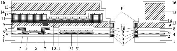
wherein the backplane film layer further comprises a buffer layer, an active layer, a gate insulating layer, a gate layer, an interlayer insulating layer, a source/drain layer, a passivation layer, a planarization layer, an anode layer and a pixel defining layer on the substrate in that order; wherein the buffer layer, the gate insulating layer, the interlayer insulating layer and the passivation layer are inorganic film layers; and
wherein the display panel further comprises:
a film layer of a light-emitting device disposed on a side, facing away from the substrate, of the backplane film layer; wherein the film layer of the light-emitting device is provided with a hollow area at a position of the via hole;
an encapsulation layer arranged on a side, facing away from the substrate, of the film layer of the light-emitting device; wherein the encapsulation layer comprises: a first inorganic encapsulation layer, an organic encapsulation layer and a second inorganic encapsulation layer arranged on the substrate in sequence along a direction of ascending distance from the substrate; wherein the second inorganic encapsulation layer is provided with an inclined part, wherein the inclined part extends towards the backplane film layer on a side facing towards the via hole; and a section of the inclined part is step-like and covers in sequence a side wall of the organic encapsulation layer, a side wall of the first inorganic encapsulation layer and part of the backplane film layer; and
an encapsulating protective barrier arranged on a side, facing away from the substrate, of the protective barrier, wherein the encapsulating protective barrier covers the inclined part and is in contact with the inclined part.
|