| CPC H10K 59/60 (2023.02) [G06N 3/02 (2013.01); H04N 7/144 (2013.01); H01L 27/1225 (2013.01); H01L 27/14612 (2013.01)] | 16 Claims |
|
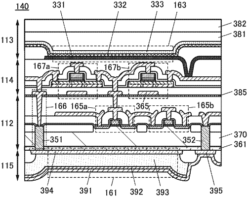
1. A semiconductor device comprising:
a photoelectric conversion element;
an insulating layer over the photoelectric conversion element;
a substrate over the insulating layer;
a conductive layer in the insulating layer and the substrate;
a first transistor and a second transistor over the substrate;
a light-emitting element over the first transistor and the second transistor; and
a third transistor between the first substrate and the first transistor,
wherein the photoelectric conversion element is electrically connected to the first transistor through the conductive layer,
wherein the light-emitting element is electrically connected to the second transistor,
wherein the light-emitting element and the first transistor overlap with each other, and
wherein the first transistor and the photoelectric conversion element overlap with each other.
|