| CPC H10K 59/38 (2023.02) [H01L 27/156 (2013.01); H01L 33/08 (2013.01); H10K 59/124 (2023.02); H10K 59/1213 (2023.02); H10K 71/00 (2023.02)] | 9 Claims |
|
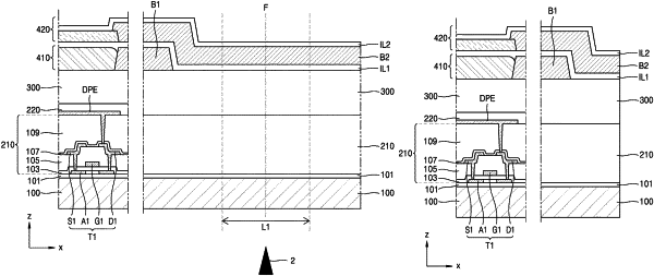
1. A method of manufacturing a display apparatus, the method comprising:
forming, on a substrate, a bottom metal layer, a pixel circuit layer including a thin-film transistor having a semiconductor layer overlapping the bottom metal layer, and a blocking layer;
forming, on the pixel circuit layer, a display element layer including a display element electrically connected to the thin-film transistor;
forming, on the display element layer, a color filter layer including a color filter overlapping the display element and a black matrix having a first side contacting the color filter and a second side extending in an edge direction of the substrate; and
cutting the substrate and the black matrix at a tip end of the blocking layer, the tip end being at the second side of the black matrix.
|