| CPC H10B 63/24 (2023.02) [H10N 70/841 (2023.02); H10N 70/8828 (2023.02)] | 17 Claims |
|
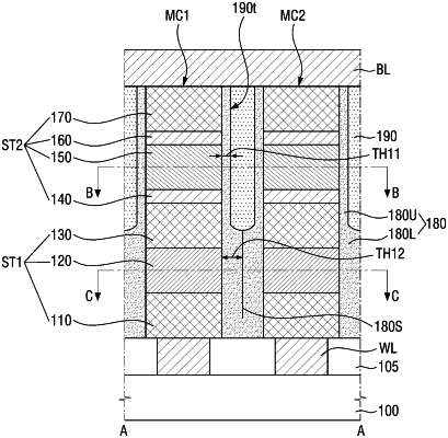
1. A semiconductor memory device comprising:
a first memory cell provided on a substrate;
a second memory cell provided on the substrate and spaced apart from the first memory cell;
a passivation layer extending along a side surface of the first memory cell and a side surface of the second memory cell; and
a gap fill layer covering the passivation layer,
wherein each of the first memory cell and the second memory cell comprises:
a selection pattern having ovonic threshold switching characteristics; and
a storage pattern provided on the selection pattern, wherein the passivation layer comprises:
a lower portion filling a space between the selection pattern of the first memory cell and the selection pattern of the second memory cell; and
an upper portion extending along a side surface of the storage pattern of each of the first memory cell and the second memory cell,
wherein the gap fill layer is not interposed between the selection pattern of the first memory cell and the selection pattern of the second memory cell,
wherein the gap fill layer is interposed between the storage pattern of the first memory cell and the storage pattern of the second memory cell, and
wherein the gap fill layer comprises a material having a lower thermal conductivity than the passivation layer.
|