| CPC H10B 61/20 (2023.02) [H03K 19/20 (2013.01); H10B 61/10 (2023.02); H10B 63/30 (2023.02)] | 6 Claims |
|
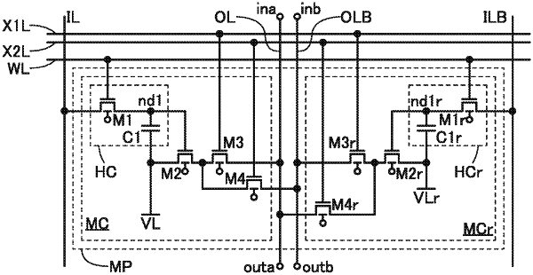
1. A semiconductor device comprising a first circuit and a second circuit,
the first circuit comprises:
first to fourth transistors; and
a first capacitor,
the second circuit comprises:
fifth to eighth transistors; and
a second capacitor,
wherein a first terminal of the first transistor is electrically connected to a gate of the second transistor,
wherein a first terminal of the second transistor is electrically connected to a first terminal of the third transistor and a first terminal of the fourth transistor,
wherein the first terminal of the third transistor is electrically connected to the first terminal of the fourth transistor,
wherein a second terminal of the third transistor is electrically connected to a first wiring,
wherein a gate of the third transistor is electrically connected to a first input wiring,
wherein a second terminal of the fourth transistor is electrically connected to a second wiring, and
wherein a gate of the fourth transistor is electrically connected to a second input wiring.
|