| CPC H10B 61/10 (2023.02) [H10N 50/80 (2023.02); G11C 11/161 (2013.01); H10N 50/85 (2023.02)] | 10 Claims |
|
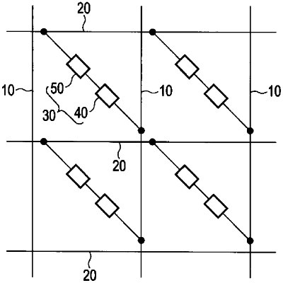
1. A non-volatile memory storage device, comprising:
a plurality of lower wiring lines extending in a first direction and spaced from one another in a second direction at a first pitch;
a plurality of upper wiring lines extending in the second direction and spaced from one another in the first direction at the first pitch; and
a plurality of memory cells, each memory cell being at an intersection between a lower wiring line and an upper wiring line, each memory cell including a resistance change element and a selector connected in series between the lower wiring line and the upper wiring line, wherein
memory cells respectively connected to each lower wiring line in the plurality of lower wiring lines are aligned with each other along a centerline of the respective lower wiring line at a first pitch, and
memory cells respectively connected to each upper wiring line in the plurality of upper wiring lines are aligned with either a first edge of the upper wiring line or a second edge of the respective upper wiring line, the first edge and the second edge being spaced from each other in the first direction, and adjacent memory cells connected to the same upper wiring line being on opposite ones of the first or second edge.
|