| CPC H10B 53/30 (2023.02) [H01L 28/60 (2013.01)] | 20 Claims |
|
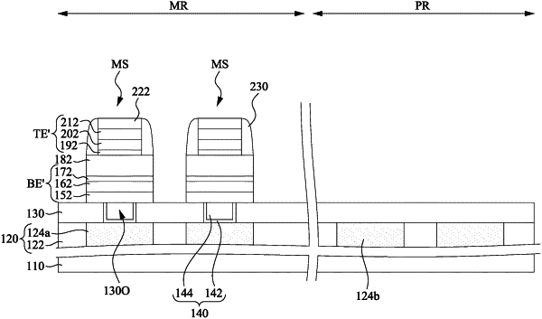
1. A method for fabricating a semiconductor device, comprising:
depositing a bottom electrode layer over a substrate;
depositing a ferroelectric layer over the bottom electrode layer;
depositing a noble metal layer over the ferroelectric layer;
depositing a non-noble metal layer over the noble metal layer, wherein the non-noble metal layer is free of noble metal; and
removing portions of the non-noble metal layer, the noble metal layer, the ferroelectric layer, and the bottom electrode layer to form a memory stack, the memory stack comprising remaining portions of the non-noble metal layer, the noble metal layer, the ferroelectric layer, and the bottom electrode layer.
|