| CPC H10B 51/20 (2023.02) [H01L 29/0649 (2013.01); H10B 51/10 (2023.02)] | 20 Claims |

|
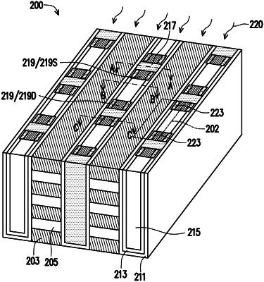
1. A method of forming a three-dimensional (3D) memory device, the method comprising:
forming a layer stack over a substrate, the layer stack comprising alternating layers of a first conductive material and a first dielectric material;
forming trenches extending vertically through the layer stack from an upper surface of the layer stack distal from the substrate to a lower surface of the layer stack facing the substrate, wherein the trenches separate the layer stack into a plurality of fin-shaped structures;
lining sidewalls and bottoms of the trenches with a memory film;
forming a channel material over the memory film, the channel material comprising an amorphous material;
filling the trenches with a second dielectric material after forming the channel material;
forming memory cell isolation regions in the second dielectric material, comprising:
forming openings in the second dielectric material between a first fin-shaped structure and a second fin-shaped structure, wherein the openings extend vertically through the second dielectric material and the channel material, wherein the openings expose a first sidewall of the memory film extending along a first sidewall of the first fin-shaped structure, and expose a second sidewall of the memory film extending along a second sidewall of a second fin-shaped structure; and
filling the openings with a third dielectric material, wherein the third dielectric material contacts and extends along the first sidewall of the memory film and the second sidewall of the memory film;
forming source lines (SLs) and bit lines (BLs) that extend vertically in the second dielectric material on opposing sides of the memory cell isolation regions; and
crystallizing first portions of the channel material after forming the SLs and BLs.
|