| CPC H10B 43/27 (2023.02) [G11C 7/18 (2013.01); G11C 8/14 (2013.01); H10B 41/10 (2023.02); H10B 41/27 (2023.02); H10B 41/40 (2023.02); H10B 43/10 (2023.02); H10B 43/40 (2023.02)] | 20 Claims |
|
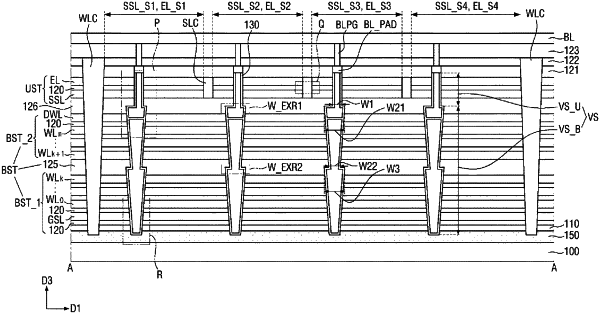
1. A semiconductor memory device comprising:
a lower stacked structure including lower metallic lines stacked in a first direction on a substrate;
an upper stacked structure including a first upper metallic line and a second upper metallic line sequentially on the lower stacked structure;
a vertical structure penetrating the upper stacked structure and lower stacked structure and including a channel film;
a connection pad disposed on the vertical structure, contacted with the channel film;
a first cutting line cutting the lower metallic lines, the first upper metallic line and the second upper metallic line;
a second cutting line spaced apart from the first cutting line in a second direction different from the first direction, and cutting the lower metallic lines, the first upper metallic line and the second upper metallic line; and
sub-cutting lines cutting the first upper metallic line and the second upper metallic line between the first cutting line and the second cutting line,
wherein the channel film includes an undoped channel region and a doping channel region doped with N-type impurities, and
the doping channel region contacts the connection pad and overlaps a part of the second upper metallic line in the second direction.
|