| CPC H10B 43/27 (2023.02) [H01L 21/76805 (2013.01); H01L 21/76816 (2013.01); H01L 21/76877 (2013.01); H01L 21/76895 (2013.01); H01L 23/5226 (2013.01); H01L 23/5283 (2013.01); H01L 23/535 (2013.01); H10B 41/27 (2023.02); H10B 41/35 (2023.02); H10B 41/41 (2023.02); H10B 43/35 (2023.02); H10B 43/40 (2023.02)] | 11 Claims |
|
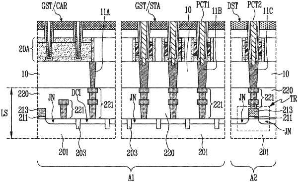
1. A method of manufacturing a semiconductor memory device, the method comprising:
forming a preliminary structure over lower contact plugs, the preliminary structure including a first semiconductor pattern and a second semiconductor pattern separated from each other by an insulating layer;
forming a stack structure including interlayer insulating layers and sacrificial layers alternately stacked on each other over the preliminary structure;
forming a channel hole and a first contact hole passing through the stack structure, wherein the channel hole overlaps the first semiconductor pattern, and wherein the first contact hole extends into an upper portion of the second semiconductor pattern;
forming a memory layer on a surface of each of the channel hole and the first contact hole;
filling the channel hole with a channel structure;
forming a first contact plug in the first contact hole, wherein the first contact plug passes through the memory layer in the first contact hole and a lower portion of the second semiconductor pattern such that the first contact plug is connected to a corresponding lower contact plug, among the lower contact plugs; and
replacing the sacrificial layers by conductive patterns,
wherein the conductive patterns surround the channel structure and the first contact plug with a corresponding memory layer interposed between each of the conductive patterns and each of the channel structure and the first contact plug.
|