| CPC H10B 43/27 (2023.02) [H10B 41/10 (2023.02); H10B 41/27 (2023.02); H10B 41/40 (2023.02); H10B 43/10 (2023.02); H10B 43/40 (2023.02)] | 20 Claims |
|
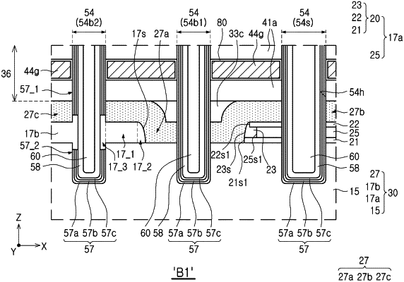
1. A semiconductor device comprising:
a pattern structure;
a stack structure on the pattern structure, the stack structure including gate layers and interlayer insulating layers alternately stacked in a vertical direction; and
a plurality of vertical structures penetrating through the stack structure in the vertical direction and in contact with the pattern structure,
wherein the pattern structure includes a lower pattern layer, an intermediate pattern layer on the lower pattern layer, and an upper pattern layer on the intermediate pattern layer,
wherein the plurality of vertical structures include a vertical memory structure penetrating through the upper pattern layer and the intermediate pattern layer and extending into the lower pattern layer,
wherein the intermediate pattern layer includes a first portion, a second portion extending from the first portion and having a decreased thickness, and a third portion extending from the first portion, having an increased thickness, and contacting the vertical memory structure, and
wherein the second portion of the intermediate pattern layer has a side surface that is curved convexly from an upper surface of the first portion of the intermediate pattern layer toward the lower pattern layer and that contacts the upper pattern layer.
|