| CPC H10B 43/27 (2023.02) [G11C 7/18 (2013.01); G11C 8/14 (2013.01)] | 18 Claims |
|
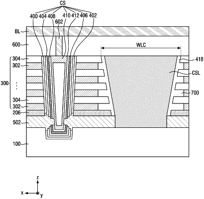
1. A nonvolatile memory device comprising:
a substrate;
a first semiconductor layer on the substrate;
an etching stop film including a metal oxide on the first semiconductor layer;
a mold structure including second semiconductor layers and insulating layers alternately stacked on the etching stop film;
a channel hole which penetrates the mold structure, the etching stop film, the first semiconductor layer and the substrate in a first direction; and
a channel structure which extends inside the channel hole and along a side wall of the channel hole, wherein the channel structure includes an anti-oxidant film on the side wall of the channel hole, a first blocking insulation film on the anti-oxidant film, a second blocking insulation film on the first blocking insulation film, a charge storage film on the second blocking insulation film, a tunnel insulating film on the charge storage film and a channel semiconductor on the tunnel insulation film,
wherein the anti-oxidant film is in contact with the second semiconductor layers,
wherein the second semiconductor layers are polysilicon,
wherein the channel semiconductor does not contact the anti-oxidant film,
wherein the first semiconductor layer penetrates the anti-oxidant film in a second direction intersecting the first direction, and directly contacts the first blocking insulation film, the second blocking insulation film, the charge storage film, and the tunnel insulating film, and
wherein the anti-oxidant film is AlN.
|