| CPC H10B 43/10 (2023.02) [H01L 25/0657 (2013.01); H01L 25/18 (2013.01); H10B 43/27 (2023.02); H01L 24/08 (2013.01); H01L 2224/08145 (2013.01); H01L 2924/1431 (2013.01); H01L 2924/14511 (2013.01)] | 19 Claims |
|
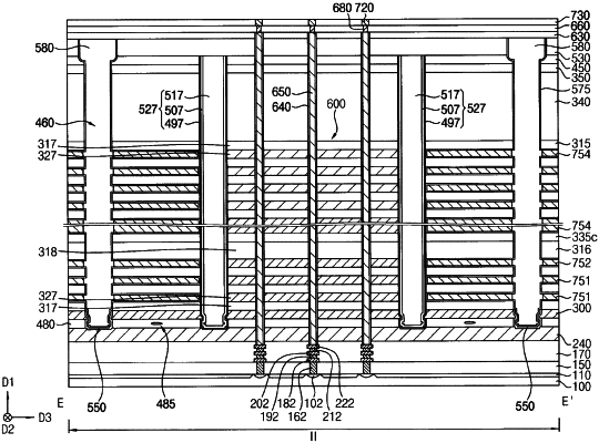
1. A semiconductor device comprising:
a gate electrode structure on a substrate, the gate electrode structure including gate electrodes spaced apart from each other in a first direction perpendicular to an upper surface of the substrate, each of the gate electrodes extending in a second direction parallel to the upper surface of the substrate;
a channel on the substrate and extending through the gate electrode structure in the first direction;
first division patterns apart from each other in the second direction, each of the first division patterns extending in the second direction through the gate electrode structure; and
a second division pattern between the first division patterns, the second division pattern and the first division patterns together dividing a first gate electrode among the gate electrodes in a third direction parallel to the upper surface of the substrate and crossing the second direction,
wherein the second division pattern has a shape in a plan view of a peanut from which opposite ends are removed, and the second division pattern overlaps ones of the gate electrodes above the first gate electrode in the first direction.
|