| CPC H10B 41/30 (2023.02) [G11C 7/18 (2013.01); G11C 8/14 (2013.01); H01L 23/5226 (2013.01); H01L 29/872 (2013.01); H10B 43/30 (2023.02)] | 20 Claims |
|
1. A memory device, comprising:
a substrate;
a first transistor and a second transistor over the substrate, wherein a first source/drain structure of the first transistor is electrically connected to a first source/drain structure of the second transistor;
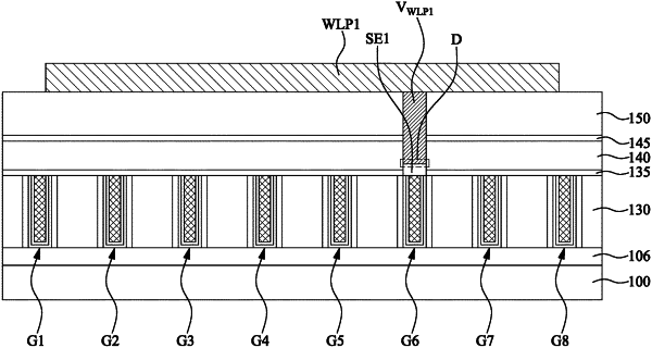
a Schottky diode electrically connected to a gate structure of the first transistor;
a first word line electrically connected to the gate structure of the first transistor through the Schottky diode;
a second word line electrically connected to a gate structure of the second transistor; and
a bit line electrically connected to a second source/drain structure of the second transistor.
|