| CPC H10B 41/27 (2023.02) [H10B 41/10 (2023.02); H10B 41/35 (2023.02); H10B 43/10 (2023.02); H10B 43/27 (2023.02); H10B 43/35 (2023.02)] | 14 Claims |
|
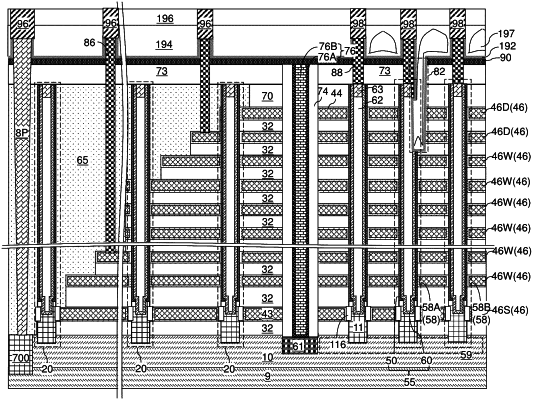
1. A three-dimensional memory device, comprising:
an alternating stack of insulating layers and electrically conductive layers located over a substrate, wherein the electrically conductive layers comprise word-line-level electrically conductive layers and drain-select-level electrically conductive layers overlying the word-line-level electrically conductive layers;
an array of memory opening fill structures located within an array of memory openings vertically extending through the alternating stack; and
a drain-select-level isolation structure vertically extending through the drain-select-level electrically conductive layers between two rows of memory opening fill structures of the array of memory opening structures and laterally extending along a first horizontal direction, and comprising a dielectric liner, a dielectric fill material portion contained within the dielectric liner, and an air gap.
|