| CPC H10B 12/34 (2023.02) [H01L 21/28088 (2013.01); H01L 21/32133 (2013.01); H01L 29/0649 (2013.01); H01L 29/4966 (2013.01); H10B 12/053 (2023.02); H10B 12/315 (2023.02)] | 20 Claims |
|
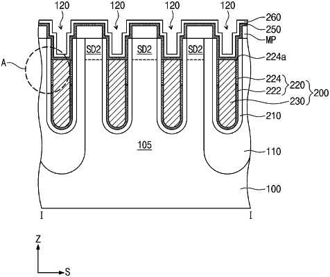
1. A semiconductor device, comprising:
a device isolation layer defining a plurality of active regions of a substrate;
a plurality gate lines intersecting the active regions and buried in the substrate;
a plurality of impurity regions in the active regions, the plurality of impurity regions comprise a first impurity region between the gate lines, and second impurity regions between the gate lines and the device isolation layer;
a bit line on the substrate and connected to the first impurity region; and
a plurality of capacitors on the substrate and connected to the second impurity regions,
wherein a gate line of the gate lines comprises:
a work-function control layer covering a sidewall of a lower portion of a trench in the substrate, the trench intersecting the active regions, and
a conductive layer filling the lower portion of the trench on the work-function control layer and including a titanium nitride,
wherein the work-function control layer comprises:
a first work-function control part surrounding a lateral surface of the conductive layer, and
a second work-function control part covering a portion of the lateral surface of the conductive layer, and disposed on the first work-function control part, and
wherein the first and second work-function control parts of the work-function control layer include a metal or metal nitride, and
wherein the second work-function control part is doped with a work-function control element.
|