| CPC H10B 12/34 (2023.02) [H01L 21/3086 (2013.01); H01L 29/0649 (2013.01); H01L 29/4236 (2013.01); H10B 12/0335 (2023.02); H10B 12/053 (2023.02)] | 20 Claims |
|
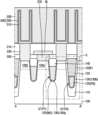
1. A semiconductor device comprising:
an active region in a substrate;
an isolation film which defines the active region in the substrate;
a gate trench which extends across the active region and the isolation film, and includes a first trench in the active region and a second trench in the isolation film;
a gate electrode which includes a main gate electrode and a pass gate electrode, the main gate electrode filling a lower part of the first trench, and the pass gate electrode filling a lower part of the second trench; and
a support structure on the pass gate electrode, the support structure filling an upper part of the second trench,
wherein a height of an upper surface of the main gate electrode from a bottom surface of the main gate electrode is greater than a height of an upper surface of the pass gate electrode from a bottom surface of the pass gate electrode, wherein a bottom surface of the pass gate electrode is lower than a bottom surface of the main gate electrode.
|