| CPC H05K 1/147 (2013.01) [G02F 1/13452 (2013.01); G06F 3/0446 (2019.05); G06F 3/04164 (2019.05); H01L 25/18 (2013.01); H05K 1/181 (2013.01); G02F 1/13338 (2013.01); H05K 2201/057 (2013.01); H05K 2201/09227 (2013.01); H05K 2201/09509 (2013.01); H05K 2201/10128 (2013.01); H05K 2201/10136 (2013.01); H10K 59/40 (2023.02)] | 21 Claims |
|
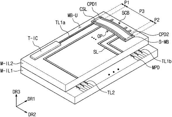
1. An apparatus, comprising:
a first circuit board including first signal lines and second signal lines;
a driving chip coupled to the first circuit board; and
a second circuit board spaced apart from and electrically connected to the driving chip, wherein the second circuit board is a flexible circuit board and wherein at least part of the second circuit board is spaced apart from a first surface of the first circuit board in a bridge structure, each of the first signal lines has different sub-lines that are spaced apart from one another and located on different insulation layers, a portion of a second insulation layer having a smaller size than a first insulation layer to expose a portion of the first insulation layer, the exposed portion of the first insulation layer including a pad area.
|