| CPC H05K 1/144 (2013.01) [H01L 25/0657 (2013.01); H05K 1/142 (2013.01)] | 19 Claims |

|
1. An electronic device comprising:
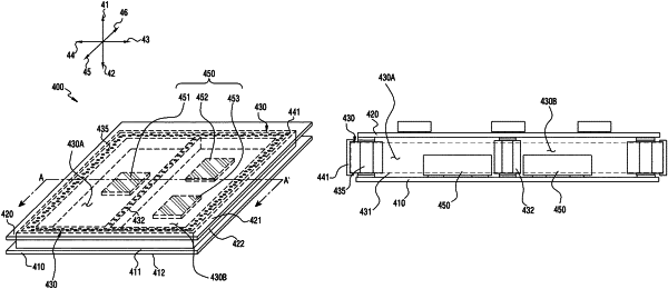
a first circuit board including a first electronic component and a second electronic component disposed on a first side of the first circuit board;
a second circuit board spaced apart from the first circuit board and having a second side facing the first side of the first circuit board; and
a first interposer disposed between the first circuit board and the second circuit board including:
a non-conductive body disposed between the first circuit board and the second circuit board,
a plurality of through holes formed through the non-conductive body, and
a plurality of conductive members disposed in the plurality of through holes for electrically connecting the first circuit board and the second circuit board,
wherein the non-conductive body includes:
a first non-conductive body having a closed-shape, and
a second non-conductive body formed straightly extending from one portion of the first non-conductive body to another portion of the first non-conductive body to provide a first inner space and a second inner space spatially isolated from each other,
wherein the first electronic component on the first circuit board is disposed corresponding to the first inner space, and the second electronic component on the first circuit board is disposed corresponding to the second inner space,
wherein a conductive portion is formed along a side surface of the second non-conductive body, the conductive portion is configured to shield the second electronic component disposed in the second inner space from the first electronic component disposed in the first inner space,
wherein the second non-conductive body includes:
a protruding portion supporting the second circuit board; and
an extension portion extended from the protruding portion and supporting a third circuit board,
wherein the electronic device further comprises:
a second interposer disposed around the first non-conductive body on the first circuit board, wherein a height of the second interposer is lower than a height of the first interposer; and
the third circuit board spaced apart from the first circuit board and disposed on an upper part of the second interposer and an upper part of the extension portion of the second non-conductive body, and
wherein the second interposer and the extension portion of the second non-conductive body are disposed between the first circuit board and the third circuit board.
|