US 11,856,279 B2
Imaging apparatus, manufacturing apparatus, manufacturing method and electronic appliance
Hidetsugu Otani, Kumamoto (JP); and Yuuji Kishigami, Kumamoto (JP)
Assigned to SONY GROUP CORPORATION, Tokyo (JP)
Filed by SONY GROUP CORPORATION, Tokyo (JP)
Filed on Oct. 10, 2022, as Appl. No. 17/962,651.
Application 17/962,651 is a continuation of application No. 16/945,129, filed on Jul. 31, 2020, granted, now 11,483,456.
Application 16/945,129 is a continuation of application No. 16/054,441, filed on Aug. 3, 2018, granted, now 10,764,479, issued on Sep. 1, 2020.
Application 16/054,441 is a continuation of application No. 14/903,110, granted, now 10,044,917, issued on Aug. 7, 2018, previously published as PCT/JP2014/071035, filed on Aug. 8, 2014.
Claims priority of application No. 2013-172536 (JP), filed on Aug. 8, 2013.
Prior Publication US 2023/0032808 A1, Feb. 2, 2023
This patent is subject to a terminal disclaimer.
Int. Cl. H04N 23/54 (2023.01); G02B 7/08 (2021.01); H04N 23/51 (2023.01); H04N 23/57 (2023.01); G03B 11/00 (2021.01); G03B 17/02 (2021.01); G02B 13/00 (2006.01); G02B 5/20 (2006.01)
CPC H04N 23/54 (2023.01) [G02B 7/08 (2013.01); H04N 23/51 (2023.01); H04N 23/57 (2023.01); G02B 5/208 (2013.01); G02B 13/001 (2013.01); G03B 11/00 (2013.01); G03B 17/02 (2013.01)] 20 Claims
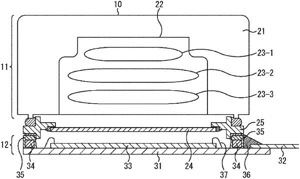
OG exemplary drawing
 
1. An imaging apparatus, comprising:
a first circuit board;
a lens configured to receive incident light;
an imaging element on a surface of the first circuit board, wherein the first circuit board is configured to receive the incident light on the surface via the lens;
a component on an outer circumference portion of the surface of the first circuit board, wherein the component is configured to process a signal received from the imaging element; and
an intermediate member configured to:
cover the component on the outer circumference portion of the surface of the first circuit board, wherein the intermediate member is in contact with at least one surface of the component, and
support the lens.