| CPC H03M 1/462 (2013.01) [H03M 1/122 (2013.01); H03M 1/1245 (2013.01); H03M 1/468 (2013.01)] | 16 Claims |
|
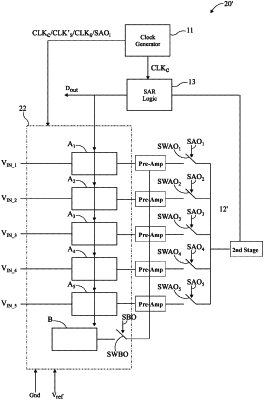
1. A successive approximation analog-to-digital converter, comprising:
a digital-to-analog converter configured to receive a digital signal, said digital-to-analog converter comprising:
first conversion units, each first conversion unit being configured to sample an analog signal via a first switch and output a first level voltage;
a single second conversion unit configured to provide a second level voltage;
wherein each first conversion unit comprises a first capacitor array and a set of said first switches controlled by the digital signal;
wherein the second conversion unit comprises a second capacitor array and a set of second switches;
a set of third switches, wherein said set of third switches comprises a third switch for each first conversion unit, each third switch configured to selectively pass the first level voltage;
a comparator configured to selectively receive the first level voltages from the set of third switches and operating to compare each received first level voltage to the second level voltage and to provide a comparison signal based on each comparison;
a successive approximation logic circuit configured to provide the digital signal based on the comparison signal generated by the comparator; and
a control circuit configured to close the first switches simultaneously and close the third switches successively for the conversion of each sampled analog signal;
wherein, for each first conversion unit, the first capacitor array comprises first capacitors, each first capacitor having a first plate connected to an output and a second plate connected through a switch to the analog signal, and, for each first capacitor, a switch connecting the second plate of the first capacitor to a first reference voltage and a switch connecting the second plate of the first capacitor to a second reference voltage;
wherein each first conversion unit further comprises a switch connecting the first plate of each first capacitor to the first reference voltage that comprises:
a first MOS transistor, the drain of the first MOS transistor receiving the first reference voltage, and the source of the first MOS transistor receiving the first level voltage;
a second MOS transistor, the source of the second MOS transistor receiving a third reference voltage, the drain of the second MOS transistor being connected to the gate of the first MOS transistor, and the gate of the second MOS transistor receiving a command signal;
a third capacitor having a first plate connected to the gate of the first MOS transistor; and
an inverter having its output connected to the second plate of the third capacitor and receiving the command signal.
|