| CPC H03K 5/08 (2013.01) [H03F 3/19 (2013.01); H03G 11/02 (2013.01); H03F 2200/294 (2013.01); H03F 2200/451 (2013.01)] | 20 Claims |
|
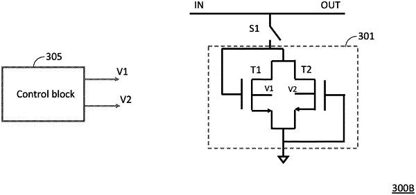
1. A radio-frequency (RF) circuit configured to feed an RF signal with an input power level from an input to an output through a terminal, the RF circuit comprising
a clamping circuit switchably connectable to the terminal, the clamping circuit being configured, in a switched-in state, to clamp the input power level of the RF signal at the terminal to an output power level lower than the input power level, the clamping circuit comprising one or more control inputs to receive control signals to adjust clamping power of the clamping circuit and select the output power level;
wherein the clamping circuit comprises a first diode-connected field effect transistor (FET) and a second diode-connected FET arranged in an antiparallel configuration, and
wherein the one or more control inputs comprise a first control input connected to a body terminal of the first diode-connected FET and a second control input connected to a body terminal of the second diode-connected FET.
|