| CPC H03K 3/42 (2013.01) | 20 Claims |
|
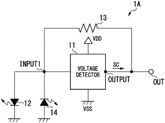
1. An optical latch circuit, comprising:
a voltage detector configured to compare a first power generation voltage input from a first input terminal with a preset first threshold voltage and start to output a set signal from a determination output terminal when the first power generation voltage exceeds the first threshold voltage;
a first photovoltaic element connected between the first input terminal and a grounding point in a forward direction in a photovoltaic mode and configured to output the first power generation voltage to the first input terminal according to photovoltaic power when light is radiated; and
a feedback resistor inserted between the first input terminal and the determination output terminal,
wherein the voltage detector is configured to only consume a power generated by the first photovoltaic element to start to output the set signal.
|