| CPC H03K 3/012 (2013.01) | 15 Claims |
|
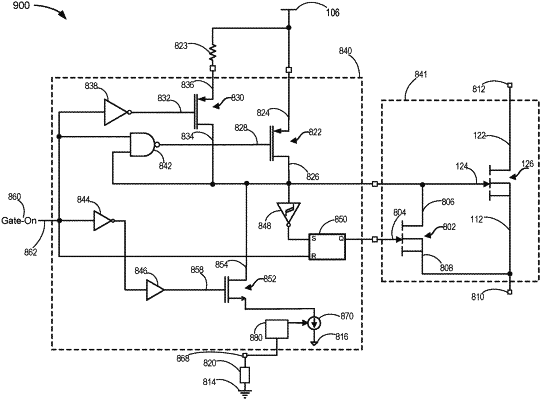
1. A circuit comprising:
a first transistor having a first gate terminal, a first source terminal and a first drain terminal;
a second transistor having a second gate terminal, a second source terminal and a second drain terminal, the second drain terminal coupled to the first gate terminal;
a control circuit coupled to the second gate terminal and arranged to change a conductive state of the second transistor in response to receiving an input signal; and
an impedance element coupled in series to the second transistor;
a detection circuit coupled to the first gate terminal;
a third transistor having a third gate terminal, a third source terminal and a third drain terminal;
a sensing circuit coupled to the impedance element and arranged to sense an impedance value of the impedance element; and
a current sink coupled to the second source terminal and to the sensing circuit;
wherein the detection circuit is coupled to the third gate terminal and the third drain terminal is coupled to the first gate terminal; and
wherein the detection circuit is arranged to sense a voltage at the first gate terminal, and in response to the voltage at the first gate terminal reaching a value below a threshold voltage, change a state of the third transistor to a conductive state.
|