| CPC H03K 19/0944 (2013.01) [H03K 17/102 (2013.01); H03K 17/687 (2013.01); H03K 19/0005 (2013.01); H03K 19/00315 (2013.01)] | 3 Claims |

|
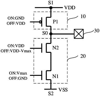
1. An asymmetrical I/O structure, comprising:
a first power supply node connected to a first voltage and a second power supply node connected to a second voltage;
a pull-up unit and a pull-down unit which are connected between the first power supply node and the second power supply node, wherein a node between the pull-up unit and the pull-down unit is connected to an I/O node;
wherein the pull-up unit comprises one or more pull-up transistors including a first pull-up transistor, the pull-down unit comprises two or more pull-down transistors including a first pull-down transistor and a second pull-down transistor connected in series, and the number of the pull-up transistors is different from the number of the pull-down transistors, and the first voltage is higher than the second voltage;
a source of the first pull-up transistor is connected to the first power supply node, a drain of the first pull-up transistor is connected to the I/O node, a gate of the first pull-up transistor is connected to an ground voltage when the first pull-up transistor is turned on, and to the first voltage when the first pull-up transistor is turned off;
a source of the first pull-down transistor is connected to the second power supply node, a drain of the first pull-down transistor is connected to a source of the second pull-down transistor, a gate of the first pull-down transistor is connected to a maximum operating voltage when the first pull-down transistor is turned on, and the gate of the first pull-down transistor is connected to the ground voltage when the first pull-down transistor is turned off;
a drain of the second pull-down transistor is connected to the I/O node, and a gate of the second pull-down transistor is connected to the maximum operating voltage, or the gate of the second pull-down transistor is connected to the first voltage when the second pull-down transistor is turned on, and the gate of the second pull-down transistor is connected to a difference voltage between the first voltage and the maximum operating voltage when the second pull-down transistor is turned off.
|