| CPC H03K 17/6872 (2013.01) [G05F 3/16 (2013.01); H01L 21/02104 (2013.01); H01L 21/283 (2013.01); H01L 21/822 (2013.01); H01L 29/0669 (2013.01); H01L 29/42312 (2013.01); H03K 19/018571 (2013.01); H03K 19/0948 (2013.01); B82Y 10/00 (2013.01)] | 20 Claims |

|
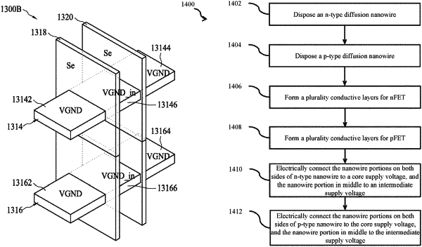
1. An integrated circuit (IC) structure, comprising:
a first diffusion nanowire, disposed on a substrate;
a second diffusion nanowire, stacked over the first diffusion nanowire along a first direction;
a plurality of first conductive layers, arranged to surround the first diffusion nanowire to form a first gate electrode, wherein the plurality of first conductive layers are arranged to extend along a second direction; and
a plurality of second conductive layers, arranged to surround the second diffusion nanowire to form a second gate electrode, wherein the plurality of second conductive layers are arranged to extend along the second direction;
wherein a first portion of the first diffusion nanowire is configured to be electrically coupled to a first reference voltage, a second portion of the second diffusion nanowire is configured to be electrically coupled to a second reference voltage, and a third portion of the first diffusion nanowire is configured to be electrically coupled to a fourth portion of the second diffusion nanowire, the first portion of the first diffusion nanowire is aligned with the second portion of the second diffusion nanowire along the first direction, and the third portion of the first diffusion nanowire is aligned with the fourth portion of the second diffusion nanowire along the first direction.
|