| CPC H03K 17/04123 (2013.01) | 19 Claims |
|
1. A switching circuit comprising:
an input terminal;
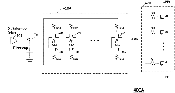
a series arrangement of main FET switches,
main gate resistors connected to corresponding gate terminals of the main FET switches, the main gate resistors being tied to one another at a main gate resistors common node;
a common bypass switch block comprising:
a series arrangement of NMOS FETs having a first NMOS FET and a second NMOS FET, the first NMOS FET being the closest to the input terminal and the second NMOS FET being the closest to the main gate resistors common node;
a series arrangement of PMOS FETs having a first PMOS FET and a second PMOS FET, the first PMOS FET being the closest to the input terminal and the second PMOS FET being the closest to the main gate resistors common node;
wherein:
drain and source terminals of the NMOS FETs are coupled with corresponding drain and source terminals of the PMOS FETs respectively;
the drain terminals of the first NMOS FET and first PMOS FET are connected together at the input terminal, and
the source terminals of the second NMOS FET and second PMOS FET are connected together at the main gate resistors common node,
the switching circuit further comprising NMOS FET gate resistors and PMOS FET gate resistors, wherein each NMOS FET gate resistor is connected to a gate terminal of a corresponding NMOS FET, and wherein each PMOS FET gate resistor is connected to a gate terminal of a corresponding PMOS FET.
|