| CPC H03H 9/02574 (2013.01) [H03H 9/02559 (2013.01); H03H 9/02834 (2013.01); H03H 9/02842 (2013.01); H03H 9/14502 (2013.01); H03H 9/14541 (2013.01); H03H 9/25 (2013.01); H03H 9/6406 (2013.01); H03H 9/725 (2013.01)] | 20 Claims |
|
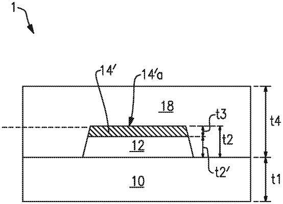
1. A method of manufacturing an acoustic wave device, the method comprising:
providing an acoustic wave device structure with one or more interdigital transducer electrode layers on a piezoelectric layer, the one or more interdigital transducer electrode layers including a conductive layer;
forming an anti-reflection layer over the conductive layer, the anti-reflection layer including silicon; and
performing a photolithography process to pattern an interdigital transducer electrode from the one or more interdigital transducer electrode layers, the anti-reflection layer reducing reflection from the conductive layer during the photolithography process.
|