| CPC H03F 1/3211 (2013.01) [H03F 3/45179 (2013.01); H03F 3/45479 (2013.01); H03F 3/4508 (2013.01); H03F 3/45085 (2013.01)] | 29 Claims |
|
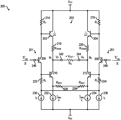
1. An electronic circuit comprising:
first and second input terminals configured to receive a differential input voltage;
first and second output terminals configured to provide a differential output voltage based on the differential input voltage;
a first supply terminal configured to receive a first supply voltage;
an input differential pair comprising:
a first transistor having a control terminal coupled to the first input terminal, and a first current path terminal coupled to the first supply terminal, and
a second transistor having a control terminal coupled to the second input terminal, and a first current path terminal coupled to the first supply terminal;
a first pair of transistors in emitter-follower configuration comprising:
a third transistor having a control terminal coupled to the first current path terminal of the first transistor, a first current path terminal coupled to the first supply terminal, and a second current path terminal coupled to the first output terminal, and
a fourth transistor having a control terminal coupled to the first current path terminal of the second transistor, a first current path terminal coupled to the first supply terminal, and a second current path terminal coupled to the second output terminal;
an output differential pair comprising:
a fifth transistor having a control terminal coupled to a second current path terminal of the first transistor, and a first current path terminal coupled to the first output terminal, and
a sixth transistor having a control terminal coupled to a second current path terminal of the second transistor, and a first current path terminal coupled to the second output terminal;
a first termination resistor coupled between the second current path terminal of the third transistor and the first current path terminal of the fifth transistor; and
a second termination resistor coupled between the second current path terminal of the fourth transistor and the first current path terminal of the sixth transistor.
|