| CPC H02S 10/30 (2014.12) [H10N 10/17 (2023.02); H10N 10/855 (2023.02)] | 11 Claims |
|
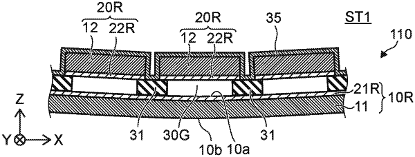
1. A power generation element, comprising:
a first conductive region including a first surface;
a plurality of second conductive regions, the second conductive regions being arranged along the first surface, a first gap being provided between the second conductive regions and the first surface the second conductive regions including a first region and a second region, the first region including a first side face, the second region including a second side face, the first side face and the second side faces crossing a plane parallel to the first surface;
a plurality of structure regions being insulating, the structure regions including a first structure region, a second structure region and a third structure region, the first structure region being provided between a part of the first region and the first surface the second structure region being provided between a part of the second region and the first surface; and
a conductive film, the conductive film including a first film region, a second film region, and a third film region, the first film region being fixed to the first side face, the second film region being fixed to the second side face, the third structure region being located between the first surface and the third film region, a second gap being provided between the first film region and the second film region; wherein in a case where a temperature of the first conductive region is higher than a temperature of the second conductive regions, electrons are emitted from the first conductive region toward the second conductive regions through the first gap.
|