| CPC H02M 1/4216 (2013.01) [H02M 1/12 (2013.01); H02M 1/4225 (2013.01); H02M 1/4233 (2013.01); H02M 7/2173 (2013.01); H02M 7/2176 (2013.01); H02M 1/42 (2013.01); H02M 7/217 (2013.01)] | 9 Claims |
|
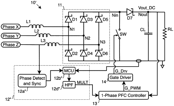
1. A power factor correction circuit, comprising:
first, second, and third phase inputs coupled to three-phase power mains;
a three-phase full-wave rectifying bridge connected to an input node;
a first boost inductor connected between a first phase input and a first tap of the three-phase full-wave rectifying bridge;
a second boost inductor connected between a second phase input and a second tap of the three-phase full-wave rectifying bridge;
a third boost inductor connected between a third phase input and a third tap of the three-phase full-wave rectifying bridge;
a boost switch connected between the input node and ground;
a boost diode connected between the input node and an output node;
a multiplier input driver configured to generate a single-phase input signal as a replica of rectified three-phase power mains, wherein the multiplier input driver comprises:
a phase detection and synchronization circuit configured to detect zero crosses of a signal at the first phase input and generate interrupts based thereupon; and
a processor receiving the interrupts and configured to generate, in cooperation with a digital to analog converter, the single-phase input signal by continuously updating an input to the digital to analog converter;
a single-phase power factor controller configured to generate a PWM signal from the single-phase input signal; and
a gate driver configured to generate a gate drive signal from the PWM signal;
wherein the boost switch is operated by the gate drive signal.
|