| CPC H01Q 5/40 (2015.01) [H01Q 5/10 (2015.01); H01Q 13/08 (2013.01); H01Q 21/24 (2013.01); H01Q 23/00 (2013.01)] | 15 Claims |
|
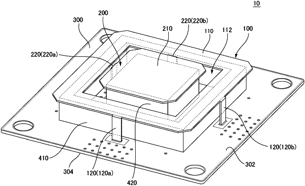
1. An antenna device comprising:
a substrate comprising a first surface;
a first element comprising a first conductive plate and a first conductive part, the first conductive plate being located at the first surface side of the substrate away from the first surface of the substrate, the first conductive plate comprising an opening, the first conductive part electrically connecting the first conductive plate and the substrate to each other; and
a second element comprising a second conductive plate and a second conductive part, the second conductive plate being located at the first surface side of the substrate away from the first surface of the substrate, the second conductive part electrically connecting the second conductive plate and the substrate to each other,
wherein the second conductive plate is located inside the opening of the first conductive plate, and
wherein the first conductive part and the second conductive part are located opposite to each other across a center of the first conductive plate or the second conductive plate.
|