| CPC H01Q 3/247 (2013.01) [H03K 17/145 (2013.01); H03K 17/567 (2013.01); H03K 17/687 (2013.01); H03K 17/693 (2013.01); H04B 1/00 (2013.01); H04B 1/48 (2013.01); H03K 17/74 (2013.01); H03K 2217/9401 (2013.01)] | 20 Claims |
|
1. A method for fabricating a semiconductor die, the method comprising:
providing a semiconductor substrate;
forming a set of field-effect transistors on the semiconductor substrate, each field-effect transistor in the set of field-effect transistors having a respective source, drain, gate, and body;
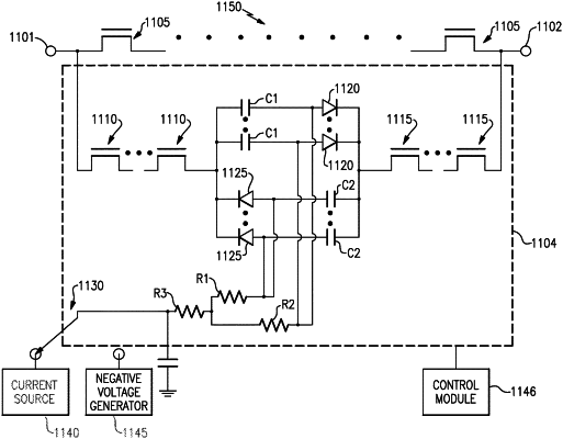
forming a compensation circuit on the semiconductor substrate, the compensation circuit including a first set of diodes coupled antiparallel to a second set of diodes, diodes in the first set of diodes parallel to each other, diodes in the second set of diodes parallel to each other, respective first capacitance directly coupled in series to each of the first set of diodes and respective second capacitance directly coupled in series to each of the second set of diodes, the first set of diodes coupled to a first resistor configured to bias the first set of diodes, the second set of diodes coupled to a second resistor configured to bias the second set of diodes, each of the first resistor and the second resistor coupled in series to a third resistor, the third resistor coupled to a first switch configured to be selectively coupled to a current source when the set of field-effect transistors are in an ON state or to a negative voltage source when the set of field-effect transistors are in an OFF state; and
connecting the compensation circuit to the set of field-effect transistors in parallel, the compensation circuit configured to compensate a non-linearity effect generated by the set of field-effect transistors.
|