| CPC H01Q 21/067 (2013.01) [H01Q 5/35 (2015.01); H01Q 5/48 (2015.01); H01Q 21/062 (2013.01)] | 20 Claims |

|
1. An antenna device comprising:
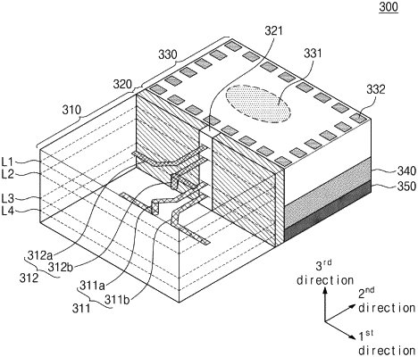
an antenna space including a first antenna configured to transmit/receive a first radio frequency (RF) signal in a first communication band and a second antenna configured to transmit/receive a second RF signal in a second communication band different from the first communication band;
a barrier including a penetration region, the barrier disposed adjacent to the antenna space and reflecting the first RF signal and the second RF signal;
a signal processing device disposed adjacent to the barrier, the signal processing device including a first RF circuit configured to process the first RF signal and a second RF circuit configured to process the second RF signal; and
a feed space comprising a first feed layer and a second feed layer, the feed space being disposed adjacent to and stacked on the signal processing device and adjacent to the barrier,
wherein a first feed line connecting the first RF circuit to the first antenna passes through the first feed layer and the penetration region of the barrier, and a second feed line connecting the second RF circuit to the second antenna passes through the second feed layer and the penetration region of the barrier.
|